The emergence of a new technology is often preceded by advances in materials science. The development of diamond technologies has borne that out since the material was first discovered. Diamond’s allure as a gemstone and its use as a tool due to its hardness have encouraged research on technical applications for centuries. Isaac Newton studied diamond, measuring its refractive index to within 1% of the currently accepted value1.
In addition to hardness, diamond has other unique properties, which include high thermal conductivity, low thermal expansion, chemical inertness, high electrical resistivity, broad optical transparency, and resistance to chemical corrosion. While many of these attributes were first identified in naturally occurring stones, recent advances in diamond synthesis have allowed researchers to begin to access diamond’s full potential.

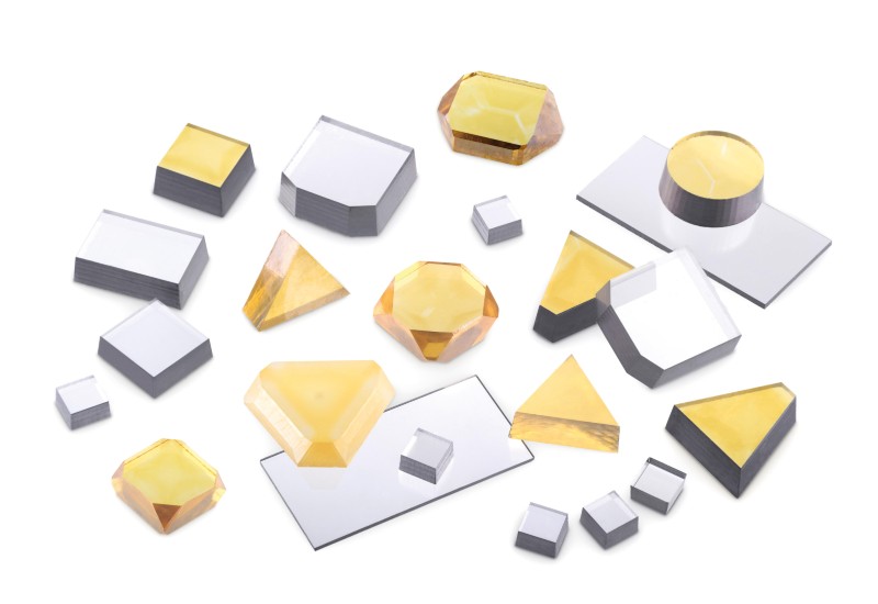
Element Six’s metallised diamond for reducing the temperature of high-power density semiconductors.
Thanks to their mass-production scale and high-quality output, high-pressure and high-temperature (HPHT) diamond and diamond-augmented tungsten carbide are the preferred materials for abrasive applications in machining, mining and construction.
An alternative synthesis method is chemical vapour deposition (CVD), which offers the potential to grow exceptionally pure diamond on a wafer scale. It also enables precision ‘doping’ with elements such as boron (in blue diamonds) for electrochemical applications, or nitrogen-vacancy (NV) in pink diamonds for quantum technology. CVD diamonds have already unlocked applications in high power lasers, EUV lithography, organic waste disposal, and sanitisation, and they continue to hold potential to disrupt the industrial ecosystem by leveraging their properties and durability.
Today, CVD diamond is used as a thermal heat spreader to manage the huge power densities (>1 kW/cm2) associated with modern semiconductor devices. Thanks to a thermal conductivity up to ten times higher than other solutions, diamond is an ideal platform on which to mount devices such as gallium nitride power amplifiers, optimising the system with junction temperatures dropping by more than 30 percent. The wide optical window of engineered single crystal CVD diamond, combined with ultra-low absorption and birefringence, have made monolithic diamond Raman lasers a commercial reality, allowing the generation of wavelengths not easily available with existing technology.

Element Six’s HPHT monocrystalline and CVD single crystal diamond, visit e6cvd.com.
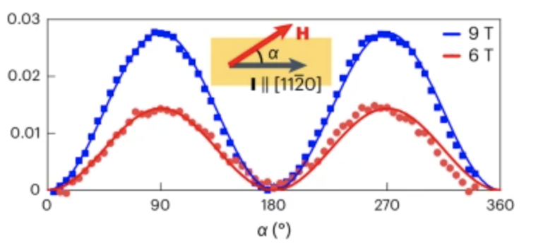
In the realm of quantum applications, the introduction of diamond nitrogen-vacancy (DNV) centres has delivered a unique solid-state platform with spin qubits that can be initialised and read out at room temperature. DNV’s superlative properties now enable high-resolution magnetic sensing for safe navigation in GPS-denied environments, while simultaneously pushing the boundaries towards cellular MRI and quantum-secure enabled networks.
Through a global network of collaborators, Element Six’s engineered NV diamond and patented technology have already accelerated the delivery of key breakthroughs in quantum research, including a Harvard study, reporting how isotopically engineered CVD single crystal reaches spin coherence times of seconds at room temperature2, and an experiment with the University of Delft, achieving the first successful loophole-free Bell’s inequality test and proving, for the first time, that ‘spooky action at a distance’ is real3.
The realisation of these breakthroughs, powered by diamond materials science, demonstrates that material scientists may have unlocked diamond’s full potential for a new generation of technology, from precision machining to semiconductors.
For more market insights, check out our latest quantum computing news here.
AUTHORS
Daniel J. Twitchen, Chief Technologist, Element Six. Contact information: [email protected]
Gabriella Sciarrone, Head of Strategic Marketing, Element Six. Contact information: [email protected]
References
- Newton I. Opticks: Or, A Treatise of the Reflections, Refractions, Inflections and Colours of Light. William Innys at the West-End of St. Paul’s (1730)
-
Maurer P. C. et al. Science. 1283-1286 (2012)
-
Hensen B. et al. Nature, 682-682 (2015)


